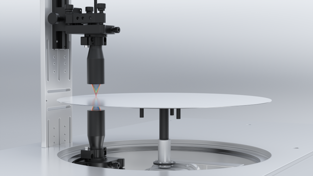
Wafer Thickness Inspection with SinceVision Spectral Confocal Displacement Sensor
Industry pain points and demands
As semiconductor technology evolves, the push for larger wafer sizes and superior quality has intensified. Even minor deviations in wafer thickness can disrupt the production process, leading to issues like chip fractures or circuit instability. These imperfections compromise the integrity of the final product, resulting in costly rework or scrapped materials.
Manufacturers require real-time, high-accuracy wafer thickness inspection to maintain consistency, reduce waste, and meet the stringent standards of modern chip fabrication. Without a reliable solution, achieving optimal quality and efficiency remains a significant challenge.
SinceVision Solutions: SCI04025 Spectral Confocal Displacement Sensor
01Unmatched Precision for Consistent Results: The SCI04025 offers a repeatability of 0.8μm, ensuring ultra-high accuracy in wafer thickness measurement. This precision minimizes variations, delivering consistent wafer quality across production batches.
02Versatile Measurement Compatibility: With a ±25° angular range and a 4μm measurement span, this spectral confocal sensor adapts seamlessly to diverse wafer surfaces, unaffected by high reflectivity, making it ideal for real-time inspections.
03Enhanced Production Efficiency: By providing reliable, high-speed thickness data, the SCI04025 helps manufacturers detect issues early, reduce defects, and streamline semiconductor processes, boosting overall productivity.
Camera Selection
| Fixture model | SCI04025 | |
| controller | SCI501A/SCI502A/SCI501B/SCI502B | |
| Fixture Model | SCI-01 | |
| Spot size | 12μm | 25.2μm |
| Measuring range | 4mm | |
| Working distance | 16mm | |
| Axial resolution | 0.006μm | |
| straightness | ±0.8μm | |
| Angle characteristic | ±25° | |
| Minimum measurable thickness of transparent object | 130μm | |
| diameter | 30mm | |
| length | 114mm | |
| weight | 95g | |


